4x4 SRAM Bank Design (Final Assignment of CMOS VLSI Circuit Design - CE 391)
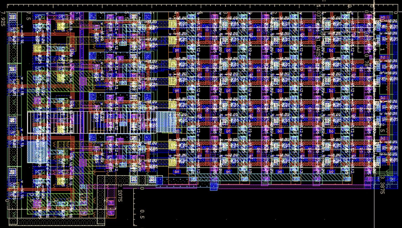
This project involved the schematic design, layout, and verification of a 4x4 SRAM array using 6T SRAM cells, integrated with essential support circuits including write drivers, clocked sense amplifiers, and bitline conditioners. Each circuit component was first designed and tested individually to ensure correct functionality and layout integrity through LVS and DRC checks.
The SRAM cell was implemented using custom sized transistors to balance stability and writeability, verified through a series of waveform simulations and post-layout extraction. A custom-designed clocked sense amplifier and write circuitry enabled correct data flow, while the bitline conditioner regulated voltage swings to optimize energy efficiency. All components were stitched together to form the SRAM Bank, with emphasis on minimal area usage.
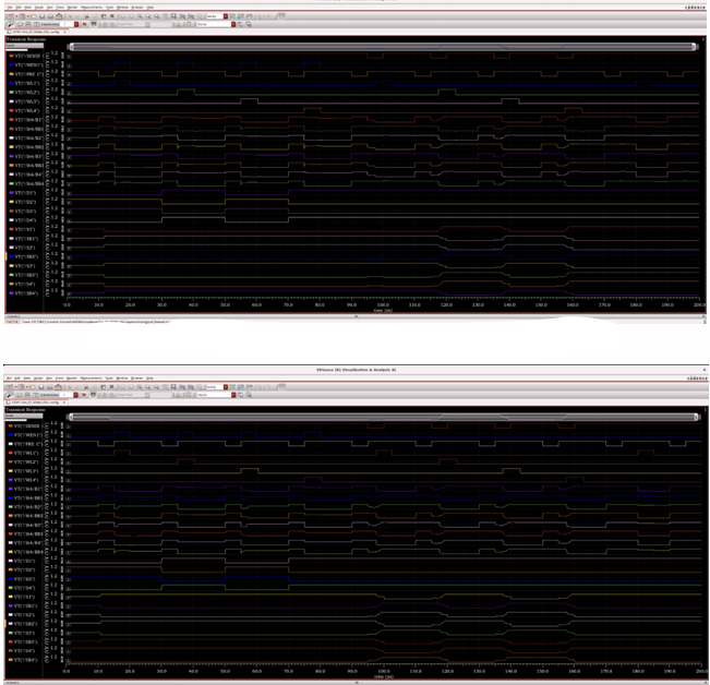
The complete system was verified at both schematic and layout levels, and simulations demonstrated correct sequential read/write behavior under clocked control at 500 MHz. Energy consumption was analyzed during read and write operations, and failure behavior was explored under increased operating frequencies up to 600 MHz. Post-layout parasitic simulations confirmed realistic performance metrics and helped identify timing bottlenecks due to sense amplifier delays.